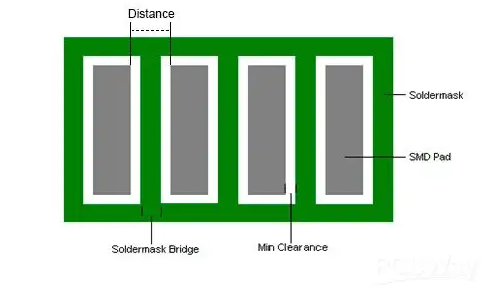
Before introducing the solder mask window, we must first know what the solder mask is. Solder mask refers to the part of the printed circuit board to be inked, which is used to cover the traces and copper to protect the metal elements on the PCB and prevent short circuits. Solder mask opening refers to opening an opening on the solder mask layer so that welding can be performed at the opening. Any location where there is no solder mask printed can be called a window opening. The location where the solder mask is not printed include soldered pads, patch pads, slot positions, and so on. There is also a case called a half-open window. The half-open window means that the pad part is not covered with solder mask, and some is covered with solder mask.
一. How to distinguish “via window” and “via cover oil”
The terms “via windowing” and “via cap oil” may be heard frequently in circuit board design. In fact, it literally means that one opens the window to the hole, and the other covers the hole with oil. In other words, whether to insulate the surface of the PCB.。
Opening the window means that it can be easily tinned at the position where the window is opened, and whether to open the window can be judged according to whether it can be tinned. Cover oil refers to the fact that it is not easy to tin during the patch, which is determined by the process. The reasons why the vias feel that they are not covered with oil are as follows: because the solder mask oil is liquid and the middle of the via holes is empty, it is easy for the oil to enter the via holes during the process of baking the solder mask oil on the solder mask ring. As a result, the yellowing of the vias occurs. This situation is related to the concentration of the solder resist oil, the oven and the strength, so there will be some cases where green can appear on it, while others cannot.
二.Why do we need to open the window for solder mask?
For vias, if the window is not opened, the ink of the solder mask will enter the hole. For some holes that do not require ink plug holes, it is necessary to design them as via holes. For through-hole mounted components, if the PCB is not soldered to open the window, the components cannot be soldered to the board normally. Aperture opening is not only a function of convenient welding, but also can be measured on vias. Solder mask openings for holes in some special positions can be used to measure the vias with a multimeter.。
For the PCB, if the window is not opened, the surface treatment cannot be performed, and neither tin spraying nor welding can be performed.
三.How to open the window for solder mask?
1. In the design, the pad will open the window by default (OVERRIDE: 0.1016mm), that is, the pad is exposed to copper foil, and the outer expansion is 0.1016mm, and the wave soldering is tinned. Design changes are not recommended to ensure solderability
2. By default, the via hole will have a window (OVERRIDE: 0.1016mm) in the design, that is, the via hole is exposed to copper foil, the external expansion is 0.1016mm, and tin will be applied during wave soldering. If the design is to prevent vias from tinning and not expose copper, the PENTING option must be checked in the additional properties of the via SOLDER MASK to close the via.
3. In addition, this layer can also be used for non-electrical wiring alone, and the solder mask green oil will open the window accordingly. If it is on the copper foil trace, it is used to enhance the overcurrent capability of the trace, and it can be tinned when soldering. If it is on a non-copper foil trace, it is usually designed for silk screen printing of logos and special characters, which can save production.
