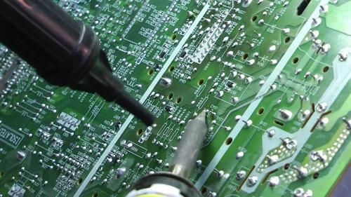
The welding of PCB is a very important link in the production process of PCB, welding will not only affect the appearance of the circuit board but also affect the performance of the circuit board. The welding points of PCB circuit board are as follows:
1. When welding PCB board, first check the model used and whether the pin position meets the requirements. When welding, first weld the two pins along the side of the opposite foot to position them, and then weld one by one from left to right.
2. Components are installed and welded in order: resistor, capacitor, diode, transistor, integrated circuit, high-power tube, other components are small first and then large.
3. When welding, there should be tin around the solder joint, and it should be firmly welded to prevent virtual welding
4. When soldering tin, tin should not be too much, when the solder joint is conical, it is the best.
5. When taking the resistance, find the required resistance, take the scissors to cut the required number of resistors, and write the resistance, so as to find
6. The chip and the base are oriented, and when welding, it is necessary to strictly follow the direction indicated by the gap on the PCB board, so that the gap of the chip, the base and the PCB correspond to each other.
7. After installing the same specification, install another specification, and try to make the height of the resistor consistent. After welding, the excess pins exposed on the surface of the printed circuit board are cut off.
8. For electrical components with too long pins (such as capacitors, resistors, etc.), cut them short after welding.
9. When the circuit is connected, it is best to clean the surface of the circuit with cleaning agent to prevent the iron filings attached to the surface of the circuit board from short-circuiting the circuit.
10. After welding, use a magnifying glass to check the solder joints and check whether there is virtual welding and short circuit.
