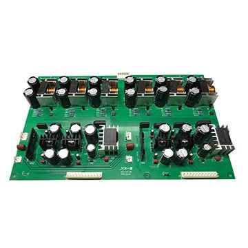
PCB design and production process has as many as 20 processes, poor tin on the circuit board may lead to such as line sandhole, wire collapse, line dog teeth, open circuit, line sand hole line; Pore copper thin serious hole without copper; If the hole copper thin is serious, the hole copper without copper; Detin is not clean (return tin times will affect the coating detin is not clean) and other quality problems, so the encounter of poor tin often means that the need to re-weld or even waste the previous work, need to be remade. Therefore, in the PCB industry, it is very important to understand the causes of poor tin
The appearance of poor tin is generally related to the cleanliness of PCB empty board surface. If there is no pollution, there will be basically no poor tin. Second, the solder itself is poor, temperature and so on. Then the printed circuit board is mainly reflected in the following points:
1. There are particle impurities in the plate coating, or there are grinding particles left on the surface of the line during the manufacturing process of the substrate.
2. Board with grease, impurities and other sundries, or there is a silicone oil residue
3. The plate surface has a sheet of electricity on the tin, the plate surface coating has particle impurities.
4. High potential coating is rough, there are plate burning phenomenon, plate surface sheet can not be on tin.。
5. The tin surface oxidation and copper surface dullness of the substrate or parts are serious.
6. One side of the coating is complete, the other side of the coating is bad, low potential hole side has obvious bright edge phenomenon.
7. Low potential holes have obvious bright edge phenomenon, high potential coating rough, there are plate burning phenomenon.
8. The welding process does not ensure adequate temperature or time, or the correct use of flux
9. Low potential large area can not be tinned, the board surface has a slight dark red or red, one side of the coating is complete, one side of the coating is bad
