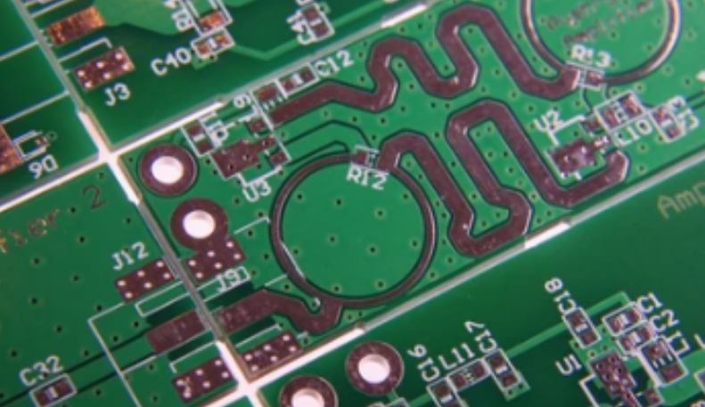
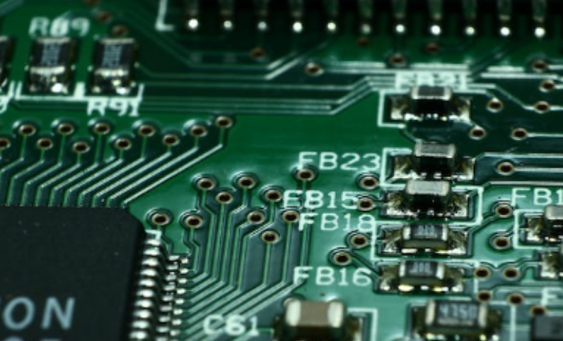
You already know that all electronic devices consist of circuit boards. PCBS, or printed circuit boards, are an integral part of today's electronics. A green board with complex lines and patterns is called a PCB. In electronic devices, markings on the PCB ensure that all components work together smoothly. The manufacturing of a PCB consists of multiple components and steps. The final stage of making a printed circuit board (PCB) is to add screen printing on the top layer.
Screen printing is the process of applying ink traces to a circuit board to identify its components, warning symbols, test points, marks, logo marks, etc. Typically, the component part is the manufacturer's screen printed side. It occasionally appears in welding channels, but the cost of getting there is high. PCB screen printing helps manufacturers and designers quickly identify component layouts. PCB screen printing will ensure that parts can be reassembled. Screen printing will provide the engineer or technician with instructions on where and how the components should be placed on the PCB.

What is PCB screen printing?
Imagine you're working on a DIY project to build a futuristic smartwatch from scratch. Your PCB is like the blueprint for this high-tech wearable, and screen printing is your way of adding intuitive marks and labels to guide you and anyone involved in the assembly process.
Screen printing on PCB is a layer of ink printed on the surface of the circuit board. It is usually made of polymer or ceramic materials and is applied through screen printing. The ink is applied through a mesh screen, which acts as a template for the desired pattern. The screen is placed on the PCB, and the ink is forced through the screen and onto the board. The standard screen colors used by manufacturers are black, yellow and white. When using PCB software, commonly used fonts can be used in the design of the screen printing layer.
It is usually applied to the top and bottom layers of the circuit board. Using screen printing, the surface of the PCB board can be printed with text, labels and symbols. Components, their location, part names, component numbers, brand logos, and other information are presented visually.
Although the screen printing layer has nothing to do with the actual electrical operation of the board, it is essential to the process of building, testing, and using the board. Helps find things and put them in the right places so that everything is lined up and in the right direction. It is very useful for the assembly process because it provides visual cues that are easy to understand for technicians and assemblers. Now that you know the basics of screen printing on printed circuit boards, let's take a look at its broader uses.

What is the information of PCB screen printing?
As mentioned earlier, screen printing on the PCB may not have any effect on the function of the PCB; However, its value lies in the information it provides. For example, it will help anyone:
Warning symbols: Identify warning symbols highlighting high-temperature components that require user attention and care during operation.
Polarity: Understand the component polarity to properly install the component. Pin markers provide directional information to ensure accurate assembly.
Test point: Position test point indicators on the screen to assist design engineers in PCB testing and commissioning.
Reference indicator: Components are identified by a reference indicator, a unique identifier for each assembly location on the PCB.
Numbers: Find a unique number on the PCB screen printing, indicating the manufacturer mark, version number, etc.
Component symbols: For special components such as diodes and optocouplers, the component symbols printed on screen printing ensure accurate alignment during installation.
Switch Settings: The default switch Settings are described on the PCB screen, enhancing the usability of the board.
Dense components: PIN on screen printing facilitates testing and debugging of compact component packages such as ball grid arrays (BGA).
Troubleshooting and repair: Silkscreen marking can easily identify and locate individual components, speeding up the repair process.
Manufacturing documentation: Silk screen marking provides the necessary manufacturing and assembly documentation. This includes copyright notices, company logos, production dates, and other important quality control and traceability details.
Brand: These marks contribute to the PCB's beauty and brand. Combining brand elements, logos, and selected colors enhances overall visual appeal and professionalism.
What is the optimal thickness of screen printing on the PCB?
The thickness of the screen on the PCB is affected by the size of the screen and the amount of ink used. In general, screen printing in PCBS is achieved as a fine coating, usually with a thickness of less than 0.1 mm. This allows the ink to be accurately applied without significantly changing the overall thickness of the PCB.
The depth of the wire mesh on a PCB can vary depending on a variety of factors, including manufacturing methods, specific requirements, and established standards within the industry. Usually, the depth of screen printing on the PCB is relatively thin compared to the other layers within the PCB.
In some cases, the thickness of the screen printed PCB layer is usually about 0.02 mm to 0.1 mm (20 to 100 microns). This is crucial to consider that these measurements are rough approximations and may vary based on a variety of factors.
Although the screen in the printed circuit board is relatively thin, it still provides plenty of visibility and elasticity for the mark. The thickness is carefully monitored to ensure that it does not disrupt the function of the PCB, trigger component misalignment, or cause complications during manufacturing.