In the layout design of the PCB, the layout of the components is crucial, which determines the neat and beautiful degree of the board and the length and quantity of the printed wire, and has a certain impact on the reliability of the whole machine.
A good circuit board, in addition to the realization of the principle of the function, but also to consider EMI, EMC, ESD (electrostatic discharge), signal integrity and other electrical characteristics, but also to consider the mechanical structure, large power chip heat dissipation problems.
General PCB layout specification requirements
1, read the design description document, meet the special structure, special module and other layout requirements.
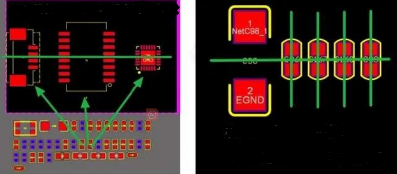
2, set the layout grid point to 25mil, can be aligned through the grid point, equal spacing; The alignment mode is large before small (large devices and large devices are aligned first), and the alignment mode is center, as shown in the following figure

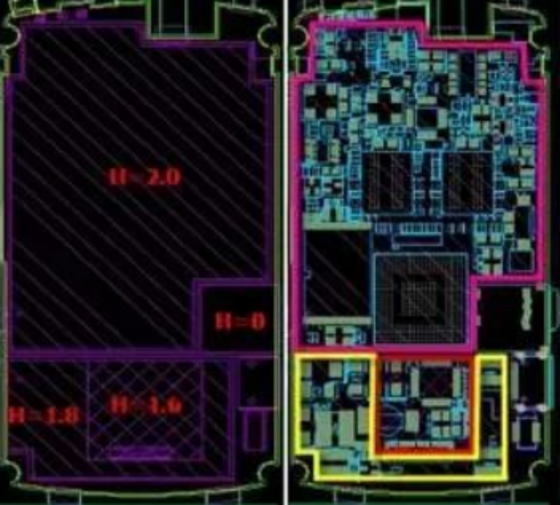
3, meet the forbidden area height limit, structure and special device layout, forbidden area requirements.
① Figure 1 (left) below: Height limit requirements, marked clearly in the mechanical layer or marking layer, convenient for later cross-check;

(2) Before layout, set the forbidden area, requiring the device to be 5mm away from the edge of the board, do not layout the device, unless special requirements or subsequent board design can add a process edge;
③ The layout of the structure and special devices can be accurately positioned by coordinates or by the coordinates of the outer frame or the center line of the components.
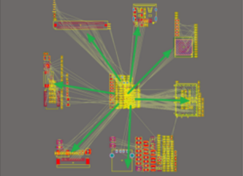
4, the layout should have a pre-layout first, do not get the board to start the layout directly, the pre-layout can be based on the module grab, in the PCB board to draw the line signal flow analysis, and then based on the signal flow analysis, in the PCB board to draw the module auxiliary line, evaluate the approximate position of the module in the PCB and the size of the occupation range. Draw the auxiliary line width 40mil, and evaluate the rationality of the layout between modules and modules through the above operations, as shown in the figure below.

5, the layout needs to consider the channel that leaves the power line, should not be too tight too dense, through the planning to figure out where the power comes from where to go, comb the power tree
6, thermal components (such as electrolytic capacitors, crystal oscillators) layout should be as far away from the power supply and other high thermal devices, as far as possible in the upper vent
7, to meet the sensitive module differentiation, the whole board layout balance, the whole board wiring channel reservation
The high-voltage and high-current signals are completely separated from the weak signals of small currents and low voltages. The high-voltage parts are hollowed out in all layers without additional copper. The creepage distance between the high-voltage parts is checked in accordance with the standard table
The analog signal is separated from the digital signal with a division width of at least 20mil, and the analog and RF are arranged in a '-' font or 'L' shape according to the requirements in the modular design
The high frequency signal is separated from the low frequency signal, the separation distance is at least 3mm, and the cross layout cannot be ensured
The layout of key signal devices such as crystal oscillator and clock driver should be far away from the interface circuit layout, not on the edge of the board, and at least 10mm away from the edge of the board. The crystal and crystal oscillator should be placed near the chip, placed in the same layer, do not punch holes, and reserve space for the ground
The same structure circuit adopts the "symmetrical" standard layout (direct reuse of the same module) to meet the consistency of the signal
After the design of the PCB, we must do analysis and inspection to make the production more smooth.