News
-

Various processes of PCBA production
The PCBA production process can be divided into several major processes: PCB design and development →SMT patch processing →DIP plug-in processing →PCBA test → three anti-coating → finished product assembly. First, PCB design and development 1.Product demand A certain scheme can obtain a certain p...Read more -

Necessary conditions for soldering PCB circuit boards
Necessary conditions for soldering PCB circuit boards 1.The weldment must have good weldability The so-called solderability refers to the performance of the alloy that the metal material to be welded and the solder can form a good combination at the appropriate temperature. Not all metals have go...Read more -
Flexible circuit board related introduction
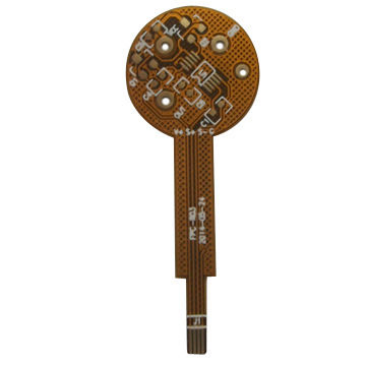
Product introduction Flexible circuit board (FPC), also known as flexible circuit board, flexible circuit board, its light weight, thin thickness, free bending and folding and other excellent characteristics are favored. However, the domestic quality inspection of FPC mainly relies on manual visu...Read more -

What are the important functions of a circuit board?
As a core component of electronic products, circuit boards have many important functions. Here are some common board features: 1. Signal transmission: The circuit board can realize the transmission and processing of signals, thereby realizing communication between electronic devices. For example...Read more -

Flexible circuit board welding method steps
1. Before welding, apply flux on the pad and treat it with a soldering iron to prevent the pad from being poorly tinned or oxidized, causing difficulty in soldering. Generally, the chip does not need to be treated. 2. Use tweezers to carefully place the PQFP chip on the PCB board, being careful n...Read more -

How to enhance the anti-static ESD function of PCB copy board?
In the design of the PCB board, the anti-ESD design of the PCB can be achieved through layering, proper layout and wiring and installation. During the design process, the vast majority of design modifications can be limited to adding or subtracting components through prediction. By adjusting the ...Read more -

How to identify the quality of PCB circuit boards?
There are many types of PCB circuit boards on the market, and it is difficult to distinguish between good and bad quality. In this regard, here are a few ways to identify the quality of PCB circuit boards. Judging from appearance 1. Appearance of weld seam Since there are many parts on the PCB c...Read more -

How to find the blind hole in the PCB board?
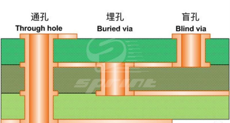
How to find the blind hole in the PCB board? In the field of electronics manufacturing, PCB (Printed Circuit Board, printed circuit board) plays a vital role, they connect and support a variety of electronic components, so that electronic devices work properly. Blind holes are a common design ele...Read more -

Procedure and precautions for double-sided circuit board welding
In the welding of two-layer circuit board, it is easy to have the problem of adhesion or virtual welding. And because of the increase of dual-layer circuit board components, each type of components for welding requirements welding temperature and so on are not the same, which also leads to the in...Read more -

PCB circuit board design and component wiring rules
The basic process of PCB circuit board design in SMT chip processing requires special attention. One of the main purposes of circuit schematic design is to provide a network table for PCB circuit board design and to prepare the basis for PCB board design. The design proc...Read more -

What is the difference between the production process of multi-layer board and double-layer board?
In general: compared with the production process of multi-layer board and double-layer board, there are 2 more processes, respectively: inner line and lamination. In detail: in the production process of double-layer plate, after the cutting is completed, drilling will be...Read more -

How to do the via and how to use the via on the PCB?
The via is one of the important components of multi-layer PCB, and the cost of drilling usually accounts for 30% to 40% of the cost of PCB board. Simply put, every hole on the PCB can be called a via. The basi...Read more
