News
-
Copper clad laminate is the core substrate
The manufacturing process of copper clad laminate (CCL) is to impregnate the reinforcing material with organic resin and dry it to form a prepreg. A blank made of several prepregs laminated together, one or both sides covered with copper foil, and a plate-shaped material formed by hot pressing. F...Read more -
Some difficult problems related to high-speed PCB, have you solved your doubts?
From PCB world 1. How to consider impedance matching when designing high-speed PCB design schematics? When designing high-speed PCB circuits, impedance matching is one of the design elements. The impedance value has an absolute relationship with the wiring method, such as walking on the su...Read more -
What development opportunities does the PCB industry have in the future?
From PCB World—- 01 The direction of production capacity is changing The direction of production capacity is to expand production and increase capacity, and to upgrade products, from the low-end to the high-end. At the same time, downstream customers should not be too concentr...Read more -
According to PCB board reinforcement materials, it is generally divided into the following types:
According to PCB board reinforcement materials, it is generally divided into the following types: 1. Phenolic PCB paper substrate Because this kind of PCB board is composed of paper pulp, wood pulp, etc., it sometimes becomes cardboard, V0 board, flame-retardant board and 94HB, etc. Its main mate...Read more -

COB soft package
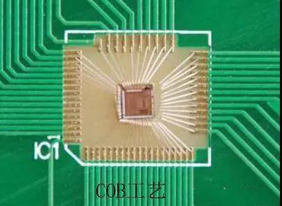
1. What is COB soft package Careful netizens may find that there is a black thing on some circuit boards, so what is this thing? Why is it on the circuit board? What is the effect? In fact, this is a kind of package. We often call it “soft package”. It is said that soft package is act...Read more -

Do you know the difference between different materials of PCB board?
–From pcb world, The combustibility of materials, also known as flame retardancy, self-extinguishing, flame resistance, flame resistance, fire resistance, flammability and other combustibility, is to evaluate the ability of the material to resist combustion. The flammable material sa...Read more -
PCB process classification
According to the number of PCB layers, it is divided into single-sided, double-sided, and multi-layer boards. The three board processes are not the same. There is no inner layer process for single-sided and double-sided panels, basically cutting-drilling-follow-up process. Multilayer boards will ...Read more -
Increase knowledge! A detailed explanation of 16 common PCB soldering defects
There is no gold, no one is perfect”, so does PCB board. In PCB welding, due to various reasons, various defects often appear, such as virtual welding, overheating, bridging and so on. This article, We explain in detail the appearance characteristics, hazards and cause analysis of 16 common...Read more -
What effect does the color of solder mask ink have on the board?
From PCB World, Many people use the color of the PCB to distinguish the quality of the board. In fact, the color of the motherboard has nothing to do with the performance of the PCB. PCB board, not that the higher the value, the easier it is to use. The color of the PCB surface is...Read more -
In PCB design, there are layout requirements for some special devices
PCB device layout is not an arbitrary thing, it has certain rules that need to be followed by everyone. In addition to general requirements, some special devices also have different layout requirements. Layout requirements for crimping devices 1) There should be no components higher than 3...Read more -
Multi-variety and small-batch PCB production
01>>The concept of multiple varieties and small batches Multi-variety, small-batch production refers to a production method in which there are many types of products (specifications, models, sizes, shapes, colors, etc.) as the production target during the specified production period, and a ...Read more -
Characteristics and discrimination of resistance damage
It is often seen that many beginners are tossing on the resistance when repairing the circuit, and it is dismantled and welded. In fact, there are a lot of repairs. As long as you understand the damage characteristics of the resistance, you don’t have to spend a lot of time. Resistor is the...Read more

