HDI: high Density interconnection of the abbreviation, high-density interconnection, non-mechanical drilling, micro-blind hole ring in the 6 mil or less, inside and outside the interlayer wiring line width / line gap in the 4 mil or less, pad diameter of not more than 0.35mm multilayer board production is called HDI board.
Blind via: short for Blind via, realizes the connection conduction between inner and outer layers.
Buried via: short for Buried via, realizing the connection between the inner layer and the inner layer.
Blind via is mostly a small hole with a diameter of 0.05mm~0.15mm, buried via is formed by laser, plasma etching and photoluminescence, and is usually formed by laser, which is divided into CO2 and YAG ultraviolet laser (UV).
HDI board material
1.HDI plate material RCC, LDPE, FR4
RCC: short for Resin coated copper, resin coated copper foil, RCC is composed of copper foil and resin whose surface has been roughened, heat-resistant, oxidation-resistant, etc., and its structure is shown in the figure below: (used when the thickness is more than 4mil)
The resin layer of RCC has the same processability as FR-1/4 bonded sheets (Prepreg). In addition to meet the relevant performance requirements of the multilayer board of the accumulation method, such as:
(1) High insulation reliability and micro-conducting hole reliability;
(2) High glass transition temperature (Tg);
(3) Low dielectric constant and low water absorption;
(4) High adhesion and strength to copper foil;
(5) Uniform thickness of insulation layer after curing.
At the same time, because RCC is a new type of product without glass fiber, it is good for etching hole treatment by laser and plasma, which is good for light weight and thinning of multilayer board. In addition, the resin coated copper foil has thin copper foils such as 12pm, 18pm, etc., which are easy to process.
Third, what is the first-order, second-order PCB?
This first-order, second-order refers to the number of laser holes, PCB core board pressure several times, playing several laser holes! Is a few orders. As shown below
1,. Pressing once after drilling holes == "the outside of the press once more copper foil == "and then laser drill holes
This is the first stage, as shown in the picture below

2, after pressing once and drilling holes == "the outside of another copper foil == "and then laser, drilling holes == "the outer layer of another copper foil == "and then laser drilling holes
This is the second order. It's mostly just a matter of how many times you laser it, that's how many steps.
Second order is then divided into stacked holes and split holes.
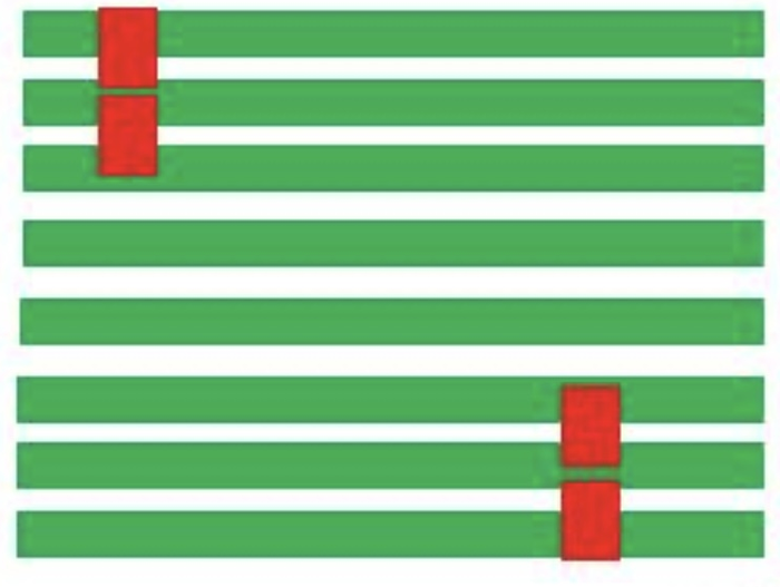
The following picture is eight layers of second-order stacked holes, is 3-6 layers first press fit, the outside of the 2, 7 layers pressed up, and hit the laser holes once. Then the 1,8 layers are pressed up and punched with laser holes once more. This is to make two laser holes. This kind of hole because it is stacked up, the process difficulty will be a little higher, the cost is a little higher.

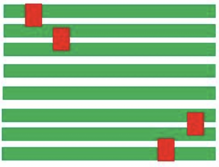
The figure below shows eight layers of second-order cross blind holes, this processing method is the same as the above eight layers of second-order stacked holes, also need to hit the laser holes twice. But the laser holes are not stacked together, the processing difficulty is much less.

Third order, fourth order and so on.