Designing any PCB is challenging, especially as devices get smaller and smaller. High-current PCB design is even more complex because it has all the same obstacles and requires an additional set of unique factors to consider.
Experts predict that the demand for high-power devices is likely to rise to achieve double-digit annual growth rates for the Industrial iot by 2030. Here are seven steps to optimize PCB design in high-current electronics for this trend.
1.Ensure sufficient cable size
Line size is one of the most important design considerations for high current PCBS. Copper wiring has tended to be miniaturized for more compact designs, but this does not work at higher currents. A small cross section can lead to power loss through heat dissipation, so a suitably large track size is required.
You can change the cross-sectional area of the wire by adjusting two factors: the width of the wire and the thickness of the copper. Balancing these two is the key to reducing power consumption and maintaining the ideal PCB size.
Use the PCB Line Width calculator to learn which widths and thicknesses support the type of current required for your device. When using these tools, be careful to design the wiring size to support higher currents than you think you need.
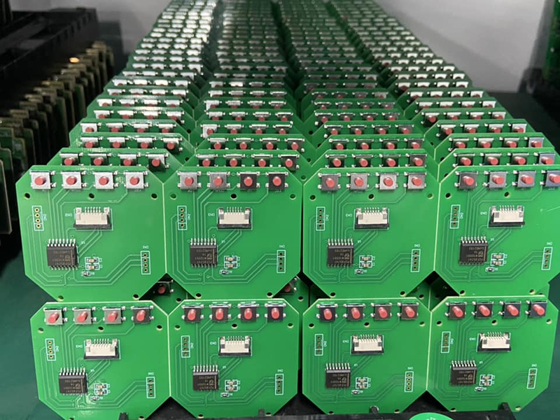
2.Rethink component placement
Component layout is another key consideration in high-current PCB design. MOSFETs and similar components generate a lot of heat, so it's important to keep them as isolated from other hot or temperature-sensitive spots as possible. This is not always easy when dealing with reduced form factors.
Amplifiers and converters should be kept at an appropriate distance from MOSFETs and other heating elements. While it may be tempting to maintain a high power zone at the edge, this does not allow for a uniform temperature distribution. Instead, they are placed in straight lines across the board to retain energy, which makes the heat more even.
By approaching the most influential areas first, it is easier to determine the ideal components. First, determine the ideal location for the high-temperature components. Once you know where to put them, you can use the rest to fill in the gaps.
3.Optimize heat dissipation management
Similarly, high current PCBS also require careful thermal management. For most applications, this means keeping the internal temperature below 130 degrees Celsius for the glass transition temperature of FR4 laminates. Optimizing component placement will help, but your heat minimization steps must stop there.
Natural convection cooling may be sufficient for smaller consumer electronics PCBS, but may not be sufficient for higher power applications. Mechanical radiators may be necessary. Active cooling such as fans or liquid cooling systems around the MOSFETs also helps. However, some device designs may not be large enough to accommodate traditional radiators or active cooling.
For smaller but high-performance PCBS, heat dissipation through holes are a useful alternative. A highly conductive metal with a series of holes poured will remove heat from MOSFETs or similar components before it reaches more sensitive areas.
4.Use the right materials
Material selection will be of great benefit when optimizing thermal management and ensuring that components can withstand higher currents. This applies to PCB components and substrates.
Although FR4 is the most common substrate, it is not always the best choice for high-current PCB designs. Metal-core PCBS may be ideal because they balance the insulation and cost-effectiveness of substrates such as FR4 with the strength and temperature displacement of highly conductive metals. Alternatively, some manufacturers make special heat-resistant laminates that you might consider.
Again, you should only use components with high thermal resistance values. Sometimes, this means choosing materials that are more heat-resistant, while in other cases it means using thicker components of the same material. Which option is best depends on your PCB size, budget, and available suppliers.
5.Improve the quality control process
The reliability of high-current PCBS is also a matter of finding errors in production. If the manufacturing process cannot find and address defects that offset its advantages, then the above four design choices will not yield much improvement. More reliable quality checks for prototype iterations are also important.
Using the right tools to evaluate the quality of a PCB is one of the most important considerations in the field. Digital optical comparators as templates and coverings outperform traditional methods as they stretch and distort over time, hindering their reliability. You should also consider tools that are easy to automate to minimize the risk of human error.
Regardless of the specific methods and techniques you use, tracking all defects is critical. Over time, this data can reveal trends in the emergence of problems, providing more reliable PCB design changes.
6.Manufacturability design
A similar but often overlooked factor in high-current PCB design is ensuring ease of manufacture. If production errors are so common that the device rarely meets the specifications on paper, it doesn't matter how reliable the PCB is in theory.
The solution is to avoid overly complex or intricate designs as much as possible. When designing high-current PCBS, keep your manufacturing process in mind, considering how these workflows might produce them and what problems might arise. The easier you can make error-free products, the more reliable they will be.
This step requires close cooperation with production stakeholders. If you don't handle manufacturing in-house, involve your production partners in the design phase to get their input on potential manufacturability issues.
7.Use technology to your advantage
New planning and production techniques can make balancing these considerations easier. 3D printing introduces more design flexibility to support more complex PCB layouts without production errors. Its precision also allows you to ensure that the copper wiring follows a curve rather than a right Angle to reduce its length and minimize power consumption
Artificial intelligence is another technology worth investigating. AI PCB tools can automatically place components or highlight potential design problems to prevent errors from appearing in the real world. Similar solutions can simulate different test environments to evaluate the performance of PCBS before producing physical prototypes.
High current PCB design requires caution
Designing a reliable high-current PCB is not easy, but it is not impossible. Following these seven steps will help you optimize your design process to create more efficient high-power devices.
As the Industrial Internet of Things grows, these considerations will become even more important. Embracing them now will be the key to continued success in the future.
