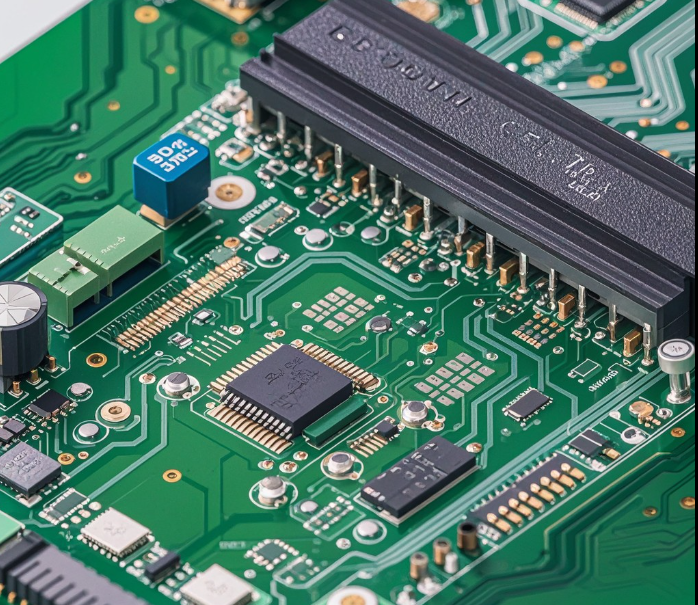
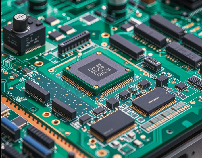
Radio frequency (RF) PCB wiring rules are one of the key factors in ensuring the performance of wireless communication devices. In high-frequency signal design, PCB wiring not only carries current, but also has a significant impact on the integrity and quality of the signal. The following is a brief analysis of the RF PCB wiring rules.
1.Impedance control
Impedance control is a core principle in RF PCB design. Typically, RF circuits have a characteristic impedance of 50 ohms, which helps maximize power transmission and reduce signal reflection. Impedance mismatches can lead to signal distortion, increased losses, and EMI problems. Impedance matching can be achieved by selecting the appropriate line width, thickness, and distance between the line and the ground layer, which need to be calculated according to the characteristics of the PCB material and the frequency being operated.
2.Cable length and width
The length and width of the track will directly affect the transmission characteristics of the signal. The track width should match the frequency of the signal and the required characteristic impedance. Too long a line may lead to signal attenuation and delay difference, while improper line width may lead to impedance discontinuity. In the design, the length of the line should be minimized, and the appropriate line width should be selected according to the frequency and PCB material characteristics.
3.Cable spacing
The spacing between RF lines should be large enough to reduce crosstalk and electromagnetic interference. Too small a pitch can increase parasitic capacitance, resulting in signal crosstalk and impedance changes. Typically, the track spacing should be at least twice the track width, but in high-density designs a larger spacing may be required to maintain signal integrity.
4.Selection of routing layer
The RF wiring should be on the outer layer of the PCB as much as possible in order to form a microstrip line structure, which helps to better control the impedance. When the lines must be in the inner layer, ensure that they are surrounded by the ground layer to form a banded line structure to reduce crosstalk and radiation.
5.Bend and Via holes
Arc transitions should be used for line bending and right Angle bending should be avoided because right angles can cause impedance mutations and signal reflections. The radius of curvature should be at least three times the width of the track to minimize impedance variation. As an interlayer connection, the existence of the hole will introduce parasitic inductance and capacitance, which will affect the signal integrity. The use of through holes should be minimized, and if they must be used, they should be used in pairs to reduce the load inductance.
6.Ground and shield
Good grounding is crucial in RF design. The ground layer should be as complete as possible, providing a clear return path for the RF signal and reducing the signal loop area, thereby reducing radiation and coupling. In multilayer board designs, it is recommended to use at least one complete ground layer.
7.Component layout
The RF component should be as close as possible to the relevant RF signal source to reduce the length of the track and potential interference. High-power circuits and sensitive low-power circuits should be arranged separately to avoid interference with each other.
8.Antenna design
For RF devices with antennas, the antenna design and feeding mode have a significant impact on system performance. The design of the antenna length, feed point and ground layer requires careful consideration to ensure efficient signal radiation and reception.
9.Decoupling and bypass
Decoupling and bypass capacitors in RF circuits are equally important for filtering noise and stabilizing the power supply. These capacitors should be as close as possible to their corresponding power supply pins and use appropriate values to cover the decoupling needs in the operating frequency range.
10.Avoid and walk on lines
Parallel RF wiring may cause strong crosstalk, resulting in degraded signal quality. If it is unavoidable, increase the distance between the cables as much as possible, and consider using ground cables for isolation.
