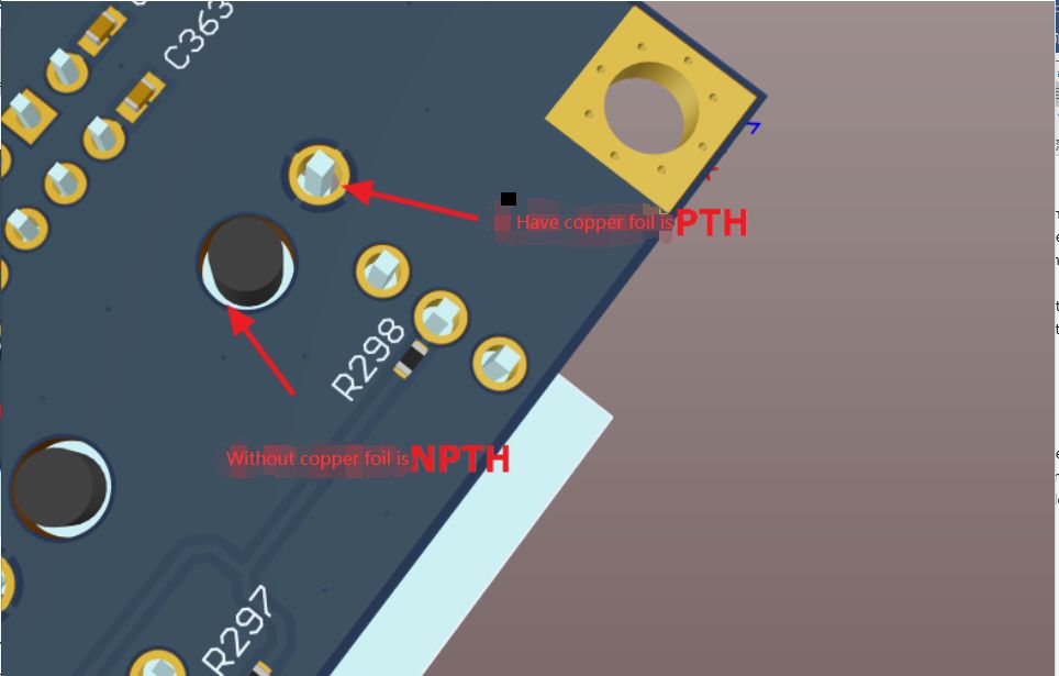
Potest animadverti multa et parva foramina in circuitu tabula, et non invenitur quod plures densa foramina et singulis foraminis disposuerat propositum. These holes can basically be divided into PTH (Plating Through Hole) and NPTH (Non Plating Through Hole) plating through hole, and we say “through hole” because it literally goes from one side of the board to the other, In fact, in addition to the through hole in the circuit board, there are other holes that are not through the circuit board.
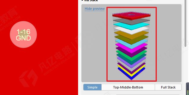
PCB Termini: per foraminis, caecus foraminis, buried foraminis.
I. Quomodo distinguantur PTH et NPTH per pertusum?
Potest iudicari si sunt clara electroplating marcas in foraminis murum. Et foraminis cum electroplating marcas est PTH, et foramen non electroplating marcas est NPTH. Sicut ostensum est in pictura infra:
II. QuodUSapiens NPTH
Non est inventus quod in apertura NPth est plerumque maior quam PTH, quia NPTh est plerumque usus est quasi cincinno screw, et quidam ad install quidam iunctio extra ad iungo fixa. Praeterea, quidam erit usus est test fixture ex parte laminam.
III. Et usus est PTH, quod via?
Plerumque, Pth foramina in circuitu tabula sunt in duobus modis. Una enim usus est ad Welding pedibus traditum intinge partes. Fortuna haec foramina maior quam diametri solutionis pedibus partium ut partes inserenda in foramina.
Another relatively small PTH, usually called via (conduction hole), is used to connect and conduction circuit board (PCB) between two or more layers of copper foil line, because PCB is composed of a lot of copper layers piled up, each layer of copper (copper) will be paved with a layer of insulation layer, that is to say, copper layer can not communicate with each other, The connection to its signal is via, which is why it is called “pass through foraminis "in Chinese. Per foramina omnino invisibilia extra. Quia per via est ad mori aeris ffoyle diversis stratis, requirit electroplating ad mores, ita per sit quaedam p.